From Schematic to PCB: A Step-by-Step Conversion Guide! Multilayer pcb-up to 48 layers manufacturing
If you are looking for Schematic To Pcb Design you've came to the right web. We have 25 Pics about Schematic To Pcb Design like Schematic To Pcb Design, How to Convert Schematic Diagram into PCB layout? - Artist 3D and also Your Guide to PCB Design Basics & Steps. Here you go:
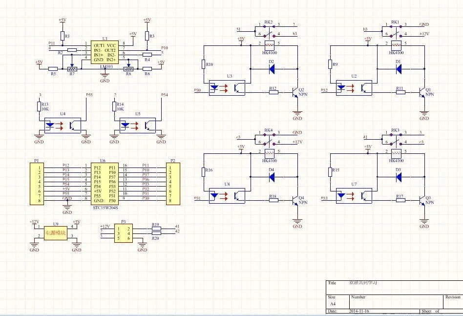
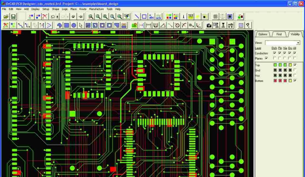
Schematic To Pcb Design
 schematicpartchar.z21.web.core.windows.net
Schematic To Pcb Design
Grams To Liters Conversion: A Step-by-Step Guide - JoyAnswer.org
 joyanswer.org
Grams to Liters Conversion: A Step-by-Step Guide - JoyAnswer.org
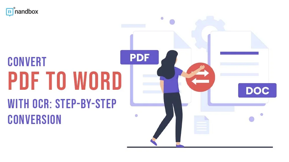
Convert PDF With OCR To Word: Step-by-Step Conversion
 nandbox.com
Convert PDF with OCR to Word: Step-by-Step Conversion
Pcb Designing How To Design A Pcb Step By Step – Artofit
 www.artofit.org
Pcb designing how to design a pcb step by step – Artofit
Pcb Designing How To Design A Pcb Step By Step – Artofit
 www.artofit.org
Pcb designing how to design a pcb step by step – Artofit
Homemade PCB: Step-By-Step Instructions For 2 Methods – Flex PCB
 flexpcb.org
Homemade PCB: Step-By-Step Instructions For 2 Methods – Flex PCB
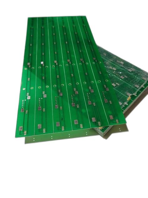
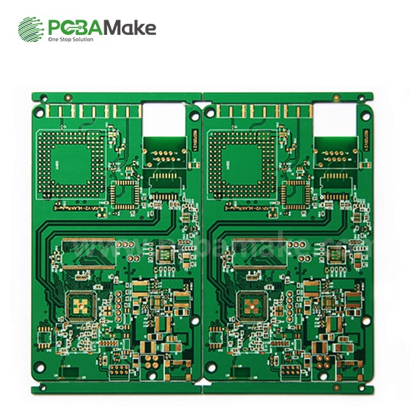
Multilayer PCB-Up To 48 Layers Manufacturing | Advanced Circuits-PcbaMake
 www.pcbamake.com
Multilayer PCB-Up To 48 Layers Manufacturing | Advanced Circuits-PcbaMake
How To 3D Print A Model Of Your PCB | Step By Step
 www.fedevel.com
How To 3D Print a Model of Your PCB | Step by Step
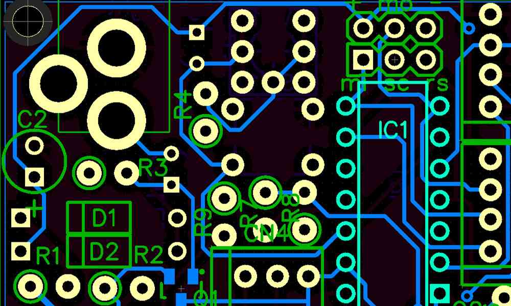
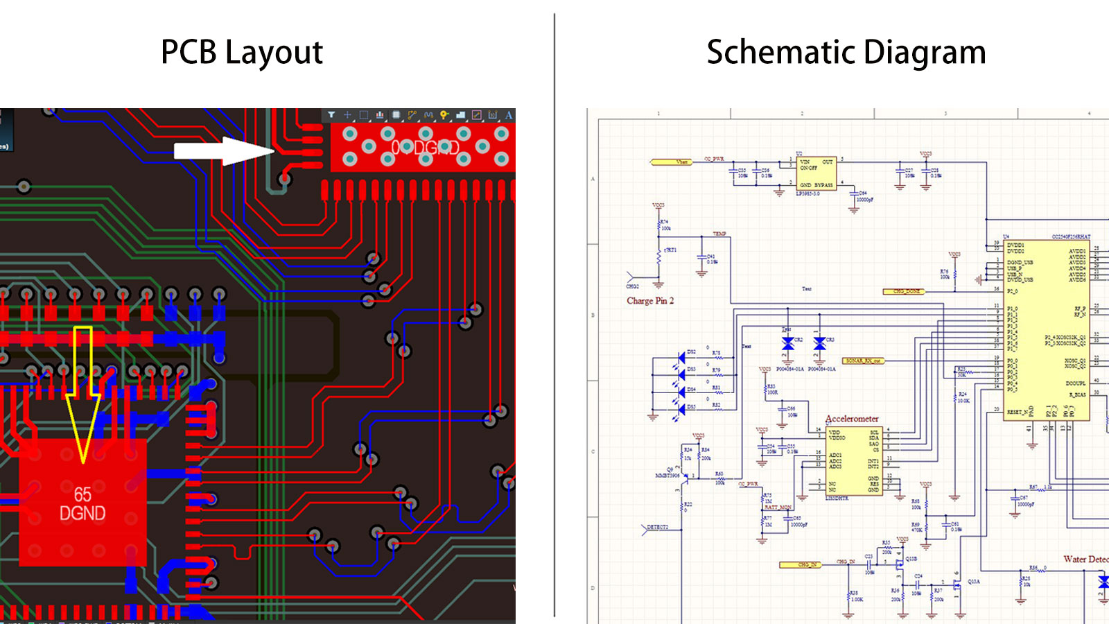
How To Convert Schematic Diagram Into PCB Layout? - Artist 3D
 artist-3d.com
How to Convert Schematic Diagram into PCB layout? - Artist 3D
How To Build A Detailed BOM (Bill Of Materials) For PCB Manufacturing
 www.victorypcb.com
How to Build a Detailed BOM (Bill of Materials) for PCB Manufacturing ...
Kicad Update Pcb From Schematic How Too Link An Existing Sch
 diagramudarim5oc.z21.web.core.windows.net
Kicad Update Pcb From Schematic How Too Link An Existing Sch
What Is The Etching Process In PCB Manufacturing?
 padpcb.com
What is the Etching Process in PCB Manufacturing?
A Complete Guide On PCB Drilling Process - JHYPCB
 www.pcbelec.com
A Complete Guide on PCB Drilling Process - JHYPCB
8 Ways To Restore PCB Schematic Diagram According To PCB Board – PCB HERO
 www.pcb-hero.com
8 Ways to Restore PCB Schematic Diagram According to PCB Board – PCB HERO
Arduino Uno Schematic Diagram: A Comprehensive Guide
 www.flux.ai
Arduino Uno Schematic Diagram: A Comprehensive Guide
Pcb Designing How To Design A Pcb Step By Step – Artofit
 www.artofit.org
Pcb designing how to design a pcb step by step – Artofit
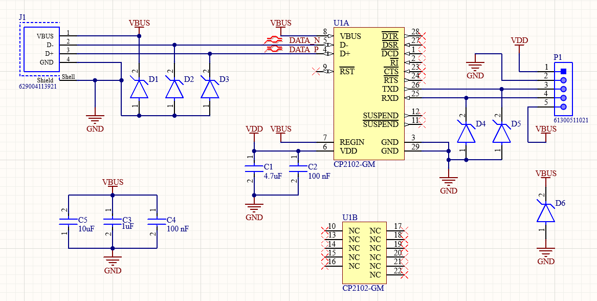
ESP32 CP2102 Programmer Schematic PCB Artists, 47% OFF
 www.oceanproperty.co.th
ESP32 CP2102 Programmer Schematic PCB Artists, 47% OFF
Pcb Designing How To Design A Pcb Step By Step – Artofit
 www.artofit.org
Pcb designing how to design a pcb step by step – Artofit
Pcb Designing How To Design A Pcb Step By Step – Artofit
 www.artofit.org
Pcb designing how to design a pcb step by step – Artofit
Pcb Designing How To Design A Pcb Step By Step – Artofit
 www.artofit.org
Pcb designing how to design a pcb step by step – Artofit
Your Guide To PCB Design Basics & Steps
 hillmancurtis.com
Your Guide to PCB Design Basics & Steps
Schematic To Pcb Converter How To Convert Schematic Pcb Layo
 lilidu73hdrcircuit.z21.web.core.windows.net
Schematic To Pcb Converter How To Convert Schematic Pcb Layo
How To Etch A PCB ? Step By Step - Artist 3D
 artist-3d.com
How to Etch a PCB ? Step by Step - Artist 3D
PCB Drilling: Comprehensive Guide For Effective Fabrication
 jamindopcba.com
PCB Drilling: Comprehensive Guide for Effective Fabrication
Pcb Designing How To Design A Pcb Step By Step Guide – Artofit
 www.artofit.org
Pcb designing how to design a pcb step by step guide – Artofit
How to convert schematic diagram into pcb layout?. Convert pdf with ocr to word: step-by-step conversion. Pcb designing how to design a pcb step by step – artofit